PTFA260851E
PTFA260851F
Confidential, Limited Internal Distribution
Thermally-Enhanced High Power RF LDMOS FET
85 W, 2500 – 2700 MHz
Description
The PTFA260851E and PTFA260851F are 85-watt LDMOS FETs
designed for WiMAX power amplifier applications in the 2500 to
2700 MHz band. Features include input and output matching, and
thermally-enhanced packages with slotted or earless flanges.
Manufactured with Infineon's advanced LDMOS process, these
devices provide excellent thermal performance and superior
reliability.
VDS = 28 V, IDQ = 900 mA
-20
2.62
GHz
2.68
GHz
2.62
15
•
Thermally-enhanced, Pb-free and RoHS-compliant packages
•
Broadband internal matching
•
Typical WiMAX performance at 2680 MHz, 28 V
- Average output power = 16 W
- Linear Gain = 14 dB
- Efficiency = 22%
- Error Vector Magnitude = –29 dB
•
Typical CW performance, 2680 MHz, 28 V
- Output power at P–1dB = 100 W
- Efficiency = 47%
-25
Efficiency
-30
10
-35
EVM
EVM (dBc)
Efficiency (%)
20
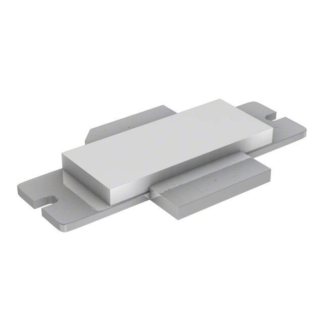
PTFA260851F
Package H-31248-2
Features
WiMAX
EVM and Efficiency vs. Output Power
25
PTFA260851E
Package H-30248-2
5
-40
•
Integrated ESD protection: Human Body Model,
Class 2 (minimum)
0
-45
•
Excellent thermal stability, low HCI drift
•
Capable of handling 10:1 VSWR @ 28 V,
85 W (CW) output power
15
20
25
30
35
40
45
Output Power (dBm)
RF Characteristics
WiMAX Measurements (not subject to production test—verified by design/characterization in Infineon test fixture)
VDD = 28 V, IDQ = 900 mA, POUT = 16 W average, ƒ = 2680 MHz, modulation = 64 QAM 2/3, channel bandwidth = 3.5 MHz,
sample rate = 4 MHz
Characteristic
Symbol
Min
Typ
Max
Unit
Gain
Gps
—
14
—
dB
Drain Efficiency
ηD
—
22
—
%
EVM
—
–29
—
dB
Error Vector Magnitude
All published data at TCASE = 25°C unless otherwise indicated
*See Infineon distributor for future availability.
ESD: Electrostatic discharge sensitive device—observe handling precautions!
Data Sheet
1 of 11
Rev. 02.1, 2009-02-20
�PTFA260851E
PTFA260851F
Confidential, Limited Internal Distribution
RF Characteristics (cont.)
Two-tone Measurements (tested in Infineon test fixture)
VDD = 28 V, IDQ = 900 mA, POUT = 85 W PEP, ƒ = 2680 MHz, tone spacing = 1 MHz
Characteristic
Symbol
Min
Typ
Max
Unit
Gain
Gps
13
14
—
dB
Drain Efficiency
ηD
33
36
—
%
IMD
—
–30
–28
dBc
Intermodulation Distortion
46.5 dBm (PEP)
DC Characteristics
Characteristic
Conditions
Symbol
Min
Typ
Max
Unit
Drain-Source Breakdown Voltage
VGS = 0 V, IDS = 10 mA
V(BR)DSS
65
—
—
V
Drain Leakage Current
VDS = 28 V, V GS = 0 V
IDSS
—
—
1.0
µA
VDS = 63 V, V GS = 0 V
IDSS
—
—
10.0
µA
RDS(on)
—
0.095
—
Ω
On-State Resistance
VGS = 10 V, V DS = 0.1 V
Operating Gate Voltage
VDS = 28 V, IDQ = 900 mA
VGS
2.0
2.5
3.0
V
Gate Leakage Current
VGS = 10 V, V DS = 0 V
IGSS
—
—
1.0
µA
Maximum Ratings
Parameter
Symbol
Value
Unit
Drain-Source Voltage
VDSS
65
V
Gate-Source Voltage
VGS
–0.5 to +12
V
Junction Temperature
TJ
200
°C
Total Device Dissipation
PD
437.5
W
2.5
W/°C
Above 25°C derate by
Storage Temperature Range
TSTG
–40 to +150
°C
Thermal Resistance (TCASE = 70°C, 85 W CW)
RθJC
0.4
°C/W
Ordering Information
Type and Version
Package Type
Package Description
Marking
PTFA260851E
V1
H-30248-2
Thermally-enhanced slotted flange, single-ended
PTFA260851E
PTFA260851F
V1
H-31248-2
Thermally-enhanced earless flange, single-ended
PTFA260851F
*See Infineon distributor for future availability.
Data Sheet
2 of 11
Rev. 02.1, 2009-02-20
�PTFA260851E
PTFA260851F
Confidential, Limited Internal Distribution
Typical Performance (data taken in a production test fixture)
Gain & Efficiency vs. Output Power
Two–tone Broadband Performance
VDD = 28 V, IDQ = 900 mA, ƒ = 2.68 GHz
15
50
40
Gain
13
30
12
20
Efficiency
11
10
-20
Intermodulation Distortion (dBc)
60
Drain Efficiency (%)
16
14
Gain (dB)
VDD = 28 V, IDQ = 900 mA, POUT = 42.5 W
0
10
25
30
35
40
45
50
55
3rd Order
-30
-40
5th
-50
7th
-60
2580 2600 2620 2640
Output Power (dBm)
Frequency (MHz)
Two–tone Performance, various voltages
Two–tone Broadband Performance
IDQ = 900 mA, ƒ = 2.68 GHz, tone spacing = 1 MHz
VDD = 28 V, IDQ = 900 mA, POUT = 42.5 W
10
Efficiency
0
50
-20
VDD = 26 V
45
-25
40
-30
VDD = 28 V
VDD = 32 V
35
30
25
-10
20
Input Return Loss
15
10
-20
-30
2590
2610
2630
2650
2670
2690
IM3, 5, 7 (dBc)
Gain
Drain Efficiency (%)
Gain (dB), Return Loss (dB)
20
-35
IM3
-40
-45
IM5
-50
-55
5
-60
0
2710
-65
IM7
25
30
35
40
45
50
Output Power (dBm )
Frequency (MHz)
Data Sheet
2660 2680 2700 2720
3 of 11
Rev. 02.1, 2009-02-20
�PTFA260851E
PTFA260851F
Confidential, Limited Internal Distribution
Typical Performance (cont.)
3-Carrier CDMA2000 Performance,
various voltages
Two–tone Performance, various voltages
IDQ = 900 mA, ƒ = 2.68 GHz, tone spacing = 1 MHz
IDQ = 900 mA, ƒ = 2.68 GHz, PAR = 7 dB
Efficiency
40
Drain Efficiency (%)
VDD = 26 V
VDD = 28 V
16
40
30
15
Gain
14
20
13
10
0
12
25
30
35
40
45
30
Efficiency
15
VDD = 32 V
14
20
Gain
13
10
12
0
30
50
35
40
45
50
Output Power (dBm)
Output Power (dBm)
3-Carrier CDMA2000 Performance
Adjacent Channel Power Ratio
WCDMA 3GPP Single-carrier Performance,
various voltages
VDD = 28 V, IDQ = 900 mA, ƒ = 2.68 GHz, PAR = 7 dB
IDQ = 900 mA, ƒ = 2.68 GHz, PAR = 8 dB
-30
VDD = 26 V
VDD = 28 V
40
16
VDD = 32 V
Drain Efficiency (%)
-40
ACPR (dBc)
VDD = 26 V
VDD = 28 V
Alt2 2.5 MHz
-50
Adj 35 MHz
-60
-70
30
15
20
14
Gain
10
Gain (dB)
Gain (dB)
VDD = 32 V
16
Gain (dB)
50
17
13
Efficiency
Alt1 2.5 MHz
-80
0
25
30
35
40
45
50
Output Power (dBm)
Data Sheet
12
25
30
35
40
45
Output Power (dBm)
4 of 11
Rev. 02.1, 2009-02-20
�PTFA260851E
PTFA260851F
Confidential, Limited Internal Distribution
Typical Performance (cont.)
WCDMA 3GPP 2-carrier Performance,
various voltages
WCDMA 3GPP Single-carrier Performance
IDQ = 900 mA, ƒ = 2.68 GHz, PAR = 8 dB
-30
ACPR (dBc), IM3U (dB)
Intermodulation Distortion (dBc)
-30
IDQ = 900 mA, ƒ = 2.68 GHz, PAR = 8 dB,
10 MHz spacing
-35
-40
32 V
-45
28 V
-50
ACPR
IMD 3
-35
-40
32 V
-45
-50
-55
25
30
35
40
45
25
50
30
35
40
45
Output Power (dBm)
Output Power (dBm)
WCDMA 3GPP 2-carrier Performance
Bias Voltage vs. Temperature
VDD = 28 V & 32 V, IDQ = 900 mA, ƒ = 2.68 GHz,
PAR = 8 dB, 10 MHz spacing
Voltage normalized to typical gate voltage,
series show current
16
VDD = 28 V
VDD = 32 V
15
Gain
20
14
10
13
Efficiency
0
Gain (dB)
30
Normalized Bias Voltage (V)
40
Drain Efficiency (%)
28 V
26 V
26 V
-55
30
35
40
45
1.02
0.56 A
0.93 A
1.01
1.39 A
1.00
2.78 A
0.99
4.17 A
5.56 A
0.98
6.95 A
0.97
8.34 A
0.96
0
20
40
60
80
100
Case Temperature (°C)
Output Power (dBm)
Data Sheet
0.19 A
0.95
-20
12
25
1.03
5 of 11
Rev. 02.1, 2009-02-20
�PTFA260851E
PTFA260851F
Confidential, Limited Internal Distribution
Broadband Circuit Impedance
Z Source Ω
Frequency
D
Z Load
G
S
R -->
R
jX
R
jX
2600
4.4
3.8
1.8
2.5
2620
4.4
3.9
1.8
2.7
2650
4.3
4.2
1.7
2.9
2680
4.2
4.5
1.7
3.2
2700
4.2
4.7
1.6
3.3
0 .1
2700 MHz
2700 MHz
2600 MHz
0.5
0.4
0.3
0.0
2600 MHz
DTOW ARD L OA
- W AV E LE NGT H
S T OW
A
RD G
E NE
RAT
O
0. 2
Z Load
Z Source
0.2
Z0 = 50 Ω
MHz
0.1
Z Source
Z Load Ω
See next page for circuit information
Data Sheet
6 of 11
Rev. 02.1, 2009-02-20
�PTFA260851E
PTFA260851F
Confidential, Limited Internal Distribution
Reference Circuit
C1
0.001µF
R2
1.3K V
R1
1.2K V
QQ1
LM7805
V DD
Q1
BCP56
C2
0.001µF
R3
2K V
C3
0.001µF
R4
2K V
R5
5.1K V
L1
R6
10 V
C4
10µF
35V
C5
0.01µF
VDD
R7
5.1K V
C6
4.5pF
C9
4.5pF
l7
R8
10 V
C10
1µF
C11
0.01µF
C12
10µF
50V
l8
l6
C7
4.5pF
RF_IN
l1
DUT
l2
l3
l4
C18
4.5pF
l5
l10
C8
1.5pF
l11
l12
l13
l14
RF_OUT
C17
0.1pF
l9
L2
a 2 6 0 8 5 1 e f _ b d _ 2 - 1 - 0 8
C13
4.5pF
C14
1µF
C15
0.01µF
C16
10µF
50V
Reference circuit schematic for ƒ = 2650 MHz
Circuit Assembly Information
DUT
PCB
PTFA260851E or PTFA260851F
0.76 mm [.030"] thick, εr = 4.5
LDMOS Transistor
TMM4
Microstrip
Electrical Characteristics at 2650 MHz1
Dimensions: L x W ( mm) Dimensions: L x W (in.)
l1
l2
l3
l4
l5
l6
l7
l8
l9
l10
l11 (taper)
l12
l13
l14
0.121
0.135
0.021
0.028
0.079
0.008
0.272
0.278
0.278
0.060
0.113
0.048
0.095
0.070
λ, 46.9 Ω
λ, 40.5 Ω
λ, 40.5 Ω
λ, 14.7 Ω
λ, 8.3 Ω
λ, 57.9 Ω
λ, 57.9 Ω
λ, 49.3 Ω
λ, 49.3 Ω
λ, 5.2 Ω
λ, 5.2 Ω / 49.3 Ω
λ, 49.3 Ω
λ, 49.3 Ω
λ, 49.3 Ω
7.42 x 1.52
8.20 x 1.93
1.27 x 1.93
1.60 x 7.54
4.37 x 14.66
0.51 x 1.04
16.79 x 1.04
16.89 x 1.40
16.89 x 1.40
3.28 x 24.36
6.73 x 24.36 / 1.40
2.97 x 1.40
5.84 x 1.40
4.29 x 1.40
2 oz. copper
0.292
0.323
0.050
0.063
0.172
0.020
0.661
0.665
0.665
0.129
0.265
0.117
0.230
0.169
x 0.060
x 0.076
x 0.076
x 0.297
x 0.577
x 0.041
x 0.041
x 0.055
x 0.055
x 0.959
x 0.959 / 0.055
x 0.055
x 0.055
x 0.055
1Electrical characteristics are rounded.
Data Sheet
7 of 11
Rev. 02.1, 2009-02-20
�PTFA260851E
PTFA260851F
Confidential, Limited Internal Distribution
Reference Circuit (cont.)
R5 C5
R3
QQ1
C1
R4
C2
R1
R2
C4
C9
LM
C10
L1
Q1
R6 R7 C6
RF_IN
VDD
C3
VDD
C12
C7
C11
C18
R8
C8
C17
RF_OUT
C15
VDD
C16
L2
C14
C13
a260851ef _cd_1-3-08
Reference circuit assembly diagram (not to scale)*
Component
Description
Suggested Manufacturer
P/N or Comment
C1, C2, C3
C4
C5, C11, C15
C6, C7, C9, C13,
C18
C8
C10, C14
C12, C16
C17
L1, L2
Q1
QQ1
R1
R2
R3
R4
R5, R7
R6, R8
Capacitor, 0.001 µF
Tantalum capacitor, 10 µF, 35 V
Capacitor, 0.01 µF
Ceramic capacitor, 4.5 pF
Digi-Key
Digi-Key
ATC
ATC
PCC1772CT-ND
399-1655-2-ND
200B 103
100B 4R5
Ceramic capacitor, 1.5 pF
Capacitor, 1 µF
Tantalum capacitor, 10 µF, 50 V
Ceramic capacitor, 0.1 pF
Ferrite, 8.9 mm
Transistor
Voltage regulator
Chip resistor 1.2 k-ohms
Chip resistor 1.3 k-ohms
Chip resistor 2 k-ohms
Potentiometer 2 k-ohms
Chip resistor 5.1 k-ohms
Chip resistor 10 ohms
ATC
ATC
Garrett Electronics
ATC
Elna Magnetics
Infineon Technologies
National Semiconductor
Digi-Key
Digi-Key
Digi-Key
Digi-Key
Digi-Key
Digi-Key
100B 1R5
920C105
TPSE106K050R0400
100A 0R1
BDS 4.6/3/8.9-4S2
BCP56
LM7805
P1.2KGCT-ND
P1.3KGCT-ND
P2KECT-ND
3224W-202ETR-ND
P5.1KECT-ND
P10ECT-ND
*Gerber Files for this circuit available on request
Data Sheet
8 of 11
Rev. 02.1, 2009-02-20
�PTFA260851E
PTFA260851F
Confidential, Limited Internal Distribution
Package Outline Specifications
Package H-30248-2
(45° X 2.72
[.107])
CL
4.83±0.51
[.190±.020]
D
FLANGE 9.78
[.385]
LID 9.40+0.10
–0.15
19.43 ±0.51
[.370+.004
–.006 ]
[.765±.020]
S
CL
2X R1.63
[R.064]
G
2X 12.70
[.500]
4X R1.52
[R.060]
27.94
[1.100]
19.81±0.20
[.780±.008]
1.02
[.040]
CL
SPH 1.57
[.062]
3.61±0.38
[.142±.015]
0.0381 [.0015]
-A34.04
[1.340]
2 4 8 c-a se s
h: -3 0 2 4 8 -2 _ p o _ 9 -F -0 8
Diagram Notes—unless otherwise specified:
1.
Lead thickness: 0.10 +0.051/–0.025 [.004 +.002/–.001].
2.
All tolerances ± 0.127 [.005] unless specified otherwise.
3.
Pins: D = drain, S = source, G = gate.
4.
Interpret dimensions and tolerances per ASME Y14.5M-1994.
5.
Primary dimensions are mm. Alternate dimensions are inches.
6.
Gold plating thickness:
S - flange: 2.54 micron [100 microinch] (min)
D, G - leads: 1.14 micron ± 0.38 micron [45 microinch ± 15 microinch]
Find the latest and most complete information about products and packaging at the Infineon Internet page
http://www.infineon.com/products
Data Sheet
9 of 11
Rev. 02.1, 2009-02-20
�PTFA260851E
PTFA260851F
Confidential, Limited Internal Distribution
Package Outline Specifications
Package H-31248-2
( 45° X 2.72
[.107])
C
L
2X 4.83±0.51
[.190±.020]
D
+0.10
LID 9.40 –0.15
[.370+.004
–.006 ]
FLANGE 9.78
[.385]
CL
19.43±0.51
[.765±.020]
G
4X R0.508 +0.381
–0.127
[R.020+.015
–.005]
2X 12.70
[.500]
19.81±0.20
[.780±.008]
C
L
SPH 1.57
[.062]
1.02
[.040]
0.0381 [.0015] -A-
S
3.61±0.38
[.142±.015]
20.57
[.810]
248-cases:h- 31248- 2_po
Diagram Notes—unless otherwise specified:
1.
Lead thickness: 0.10 +0.051/–0.025 [.004 +.002/–.001].
2.
All tolerances ± 0.127 [.005] unless specified otherwise.
3.
Pins: D = drain, S = source, G = gate.
4.
Interpret dimensions and tolerances per ASME Y14.5M-1994.
5.
Primary dimensions are mm. Alternate dimensions are inches.
6.
Gold plating thickness:
S - flange: 2.54 micron [100 microinch] (min)
D, G - leads: 1.14 micron ± 0.38 micron [45 microinch ± 15 microinch]
Find the latest and most complete information about products and packaging at the Infineon Internet page
http://www.infineon.com/products
Data Sheet
10 of 11
Rev. 02.1, 2009-02-20
�PTFA260851E/F
Confidential, Limited Internal Distribution
Revision History:
2009-02-20
2006-07-21, Preliminary Data Sheet
Previous Version:
Page
Subjects (major changes since last revision)
6, 7
1
Add impedance and circuit information.
Increase bandwidth from 2620 – 2680 to 2500 – 2700.
8
Fixed typing error
Data Sheet
We Listen to Your Comments
Any information within this document that you feel is wrong, unclear or missing at all?
Your feedback will help us to continuously improve the quality of this document.
Please send your proposal (including a reference to this document) to:
highpowerRF@infineon.com
To request other information, contact us at:
+1 877 465 3667 (1-877-GO-LDMOS) USA
or +1 408 776 0600 International
GOLDMOS ® is a registered trademark of Infineon Technologies AG.
Edition 2009-02-20
Published by
Infineon Technologies AG
81726 München, Germany
© Infineon Technologies AG 2009.
All Rights Reserved.
Legal Disclaimer
The information given in this document shall in no event be regarded as a guarantee of conditions or characteristics
(“Beschaffenheitsgarantie”). With respect to any examples or hints given herein, any typical values stated herein and/or
any information regarding the application of the device, Infineon Technologies hereby disclaims any and all warranties
and liabilities of any kind, including without limitation warranties of non-infringement of intellectual property rights of any
third party.
Information
For further information on technology, delivery terms and conditions and prices please contact your nearest Infineon
Technologies Office (www.infineon.com/rfpower).
Warnings
Due to technical requirements components may contain dangerous substances. For information on the types in question
please contact your nearest Infineon Technologies Office.
Infineon Technologies Components may only be used in life-support devices or systems with the express written approval of
Infineon Technologies, if a failure of such components can reasonably be expected to cause the failure of that life-support
device or system, or to affect the safety or effectiveness of that device or system. Life support devices or systems are
intended to be implanted in the human body, or to support and/or maintain and sustain and/or protect human life. If they fail, it
is reasonable to assume that the health of the user or other persons may be endangered.
Data Sheet
11 of 11
Rev. 02.1, 2009-02-20
�


 工商网监
湘ICP备2023018690号
工商网监
湘ICP备2023018690号
